Introduction
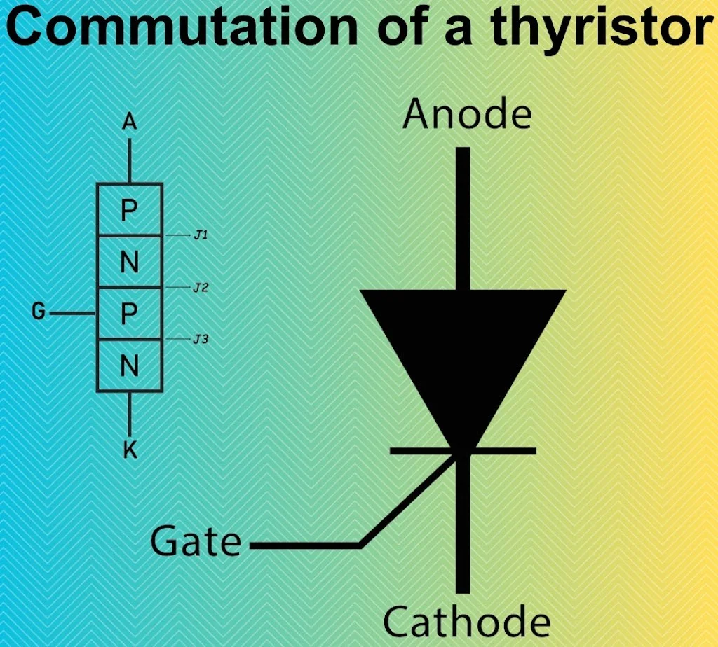
Understanding Thyristor Commutation
Types of Thyristor commutation
- In general, the term commutation refers to the process of transferring current from one path to another. More specifically, in thyristor circuits, engineers use this term to describe the act of shifting current from one thyristor to another. As previously discussed, a thyristor cannot turn itself OFF; instead, the circuit must force the current to drop to zero in order to switch it off. For this reason, engineers implement various commutation methods to achieve a controlled and timely turn-off. Consequently, these techniques ensure the safe, efficient, and reliable operation of power electronic systems. Ultimately, mastering commutation is essential for the effective design and performance of modern electrical circuits.
- Commutation forms a fundamental principle in using thyristors for control applications. A thyristor operates in only two modes: either in the OFF state (open circuit) or the ON state (short circuit). It cannot, by itself, regulate current or voltage levels in a circuit. Engineers control the circuit by adjusting the time at which the thyristor switches ON and OFF, making commutation essential to this process. All thyristor-based circuits rely on the cyclic or sequential switching of thyristors. Engineers use two main methods to commutate a thyristor, which we will now discuss.
1.Natural Commutation
- The simplest and most widely used method of commutation makes use of the alternating, reversing nature of a.c. voltages to effect the current transfer. We know that in a.c. circuits, the current always passes through zero every half cycle. As the current passes through natural zero, a reverse voltage will simultaneously appear across the device.
- This action immediately turns off the device. We call this process natural commutation because it does not require any external circuit. This method relies on AC mains supply voltages, or on AC voltages generated by local rotating machines or resonant circuits. Line-commutated converters and inverters fall under this category.
2.Forced Commutation
- Once thyristors operate in the ON state and carry forward current, you can turn them OFF only by reducing the current through them to zero for a sufficient duration to clear the charged carriers. In DC circuits, external circuits must force the forward current to zero in order to switch off the thyristors.
- We call the process forced commutation, and we refer to the external circuits used for this purpose as commutation circuits. The inductors and capacitors that make up these circuits are known as commutating components.
- A commutating circuit develops a reverse voltage across the device and immediately brings its forward current to zero, thereby turning it off. Designers face significant challenges in producing reliable commutation while developing chopper and inverter circuits. The most critical stage in the design process involves selecting a suitable forced turn-off method and determining its components.
- Engineers classify forced commutation methods based on how they arrange the commutating components and how they achieve zero current in the SCR. They use six basic commutation methods to turn OFF thyristors.
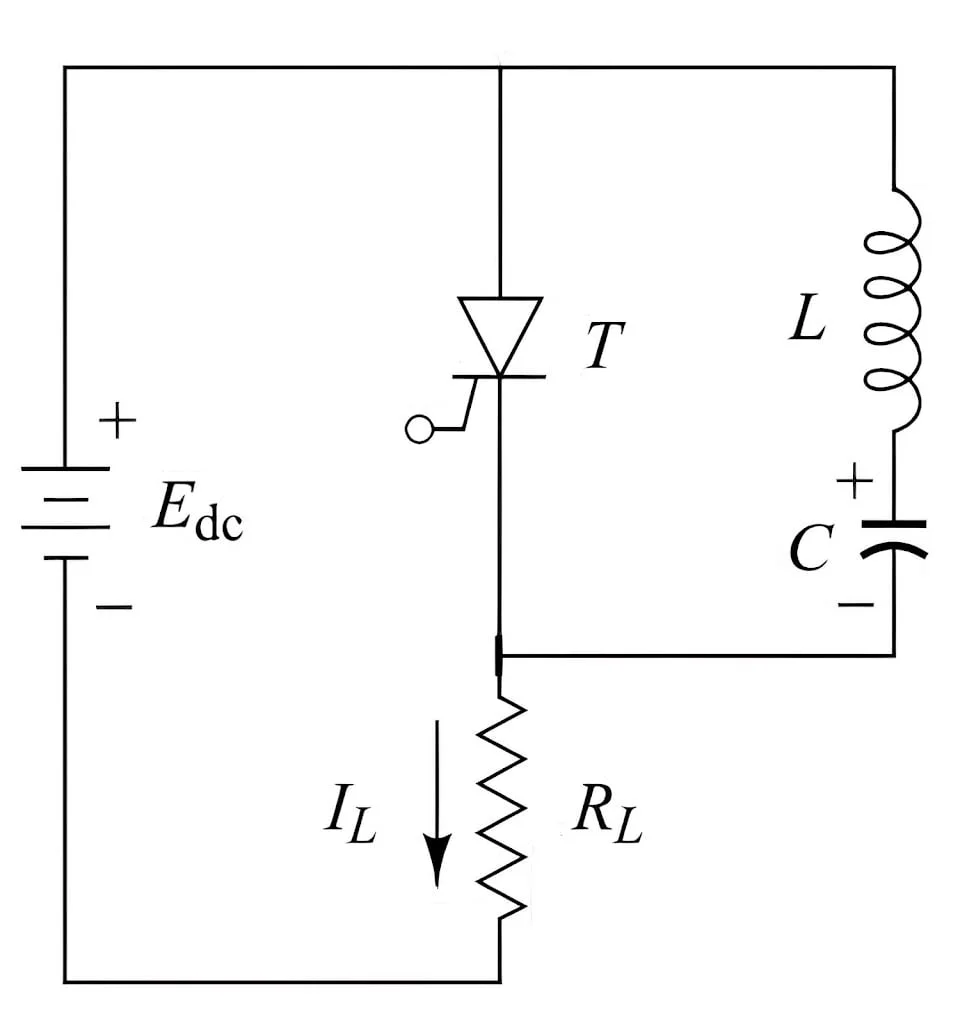
1.Class A–self Commutation by Resonating the Load
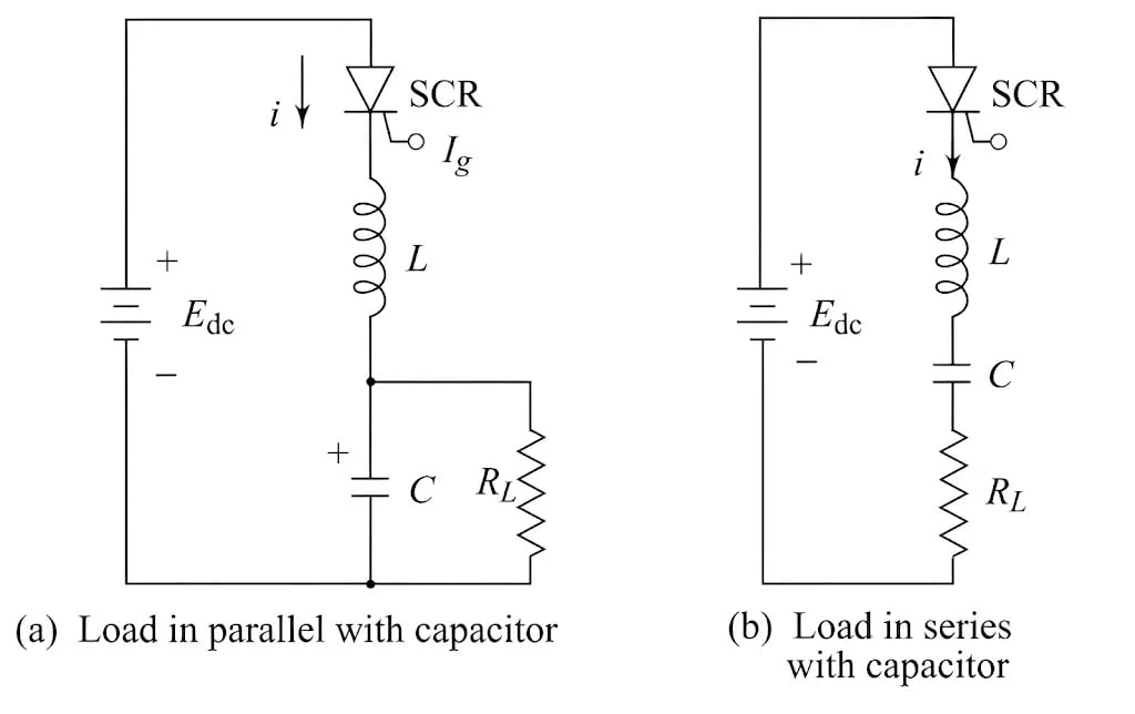
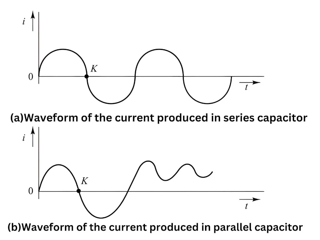
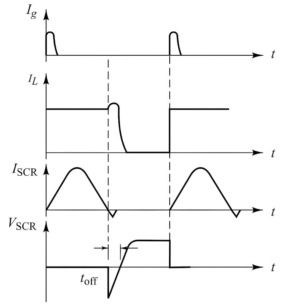
- The load resistance RL and the commutating components are so selected that their combination forms an underdamped resonant circuit. When such a circuit is excited by a d.c. source, a current of the nature shown in Fig. 2 will be obtained across the device. This current, as evident from its shape, has zero value at the point K where the device is automatically turned OFF.
- Beyond point K, the current is reversed in nature which assures definite commutation of the device.The thyristor when ON carries only the charging current of capacitor C which will soon decay to a valueless than the holding current of the device, when capacitor C is charged up to the supply voltage Edc.This simultaneously switches off the thyristor.The time for switching off the device is determined by the resonant frequency which in turn depends on the values of the commutating components L and C, and the total load resistance.
- This type of commutation circuits are most suitable for high frequency operation, i.e., above 1000 Hz, because of the need for an L-C resonant circuit which carries the full load current. This commutation circuit is used in series inverter.
2.Class B—Self Commutation by an LC Circuit
- The moment thyristor T turns ON, capacitor C discharges through the path `(C_+)`-L-T-C. Once capacitor C discharges completely, it begins charging with reverse polarity. This reverse voltage generates a commutating current `I_c` that opposes the load current `I_l`. As soon as `I_c` is greater than the load current `I_l`,the circuit turns OFF thyristor T. Afterward, capacitor C begins recharging to its original polarity through inductor L and the load. Once it becomes fully charged, the circuit turns ON the thyristor again.
- From the above discussion, we can conclude that the thyristor, after turning ON for a period, turns OFF automatically. After staying OFF for a specific duration, it turns ON again. This continuous switching between ON and OFF states repeats repeatedly. By designing the commutating components appropriately, engineers can set the desired frequency for these ON and OFF intervals. This switching process plays a key role in DC chopper circuits, where the thyristor must conduct for a set duration and then remain OFF for another defined interval.
- The Morgan chopper circuit uses a saturable reactor instead of the ordinary inductor L, forming a modified arrangement for the commutation process. This configuration offers the advantage of a longer oscillation period, which ensures more reliable commutation. In this Class B commutation method, the commutating component does not carry the load current. Both Class A and Class B turn-off circuits self-commutate, meaning the SCR turns off automatically after switching on.
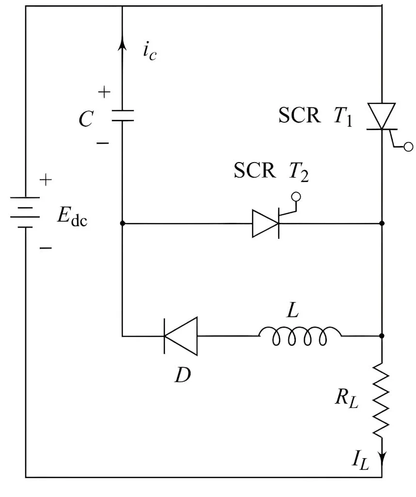
3.Class C—Complementary Commutation (Switching a Charged Capacitor by a Load Carrying SCR)
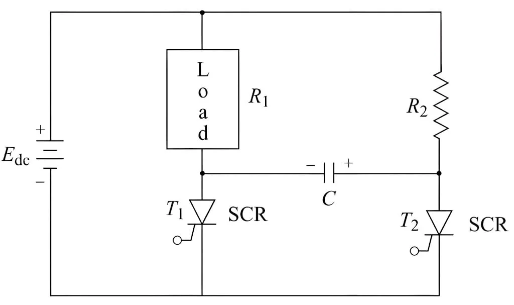
Circuit Operation
1.Mode 0: [Initial-state of circuit]
- Initially, both the thyristors are OFF.Therefore, the states of the devices are,
2.Mode 1
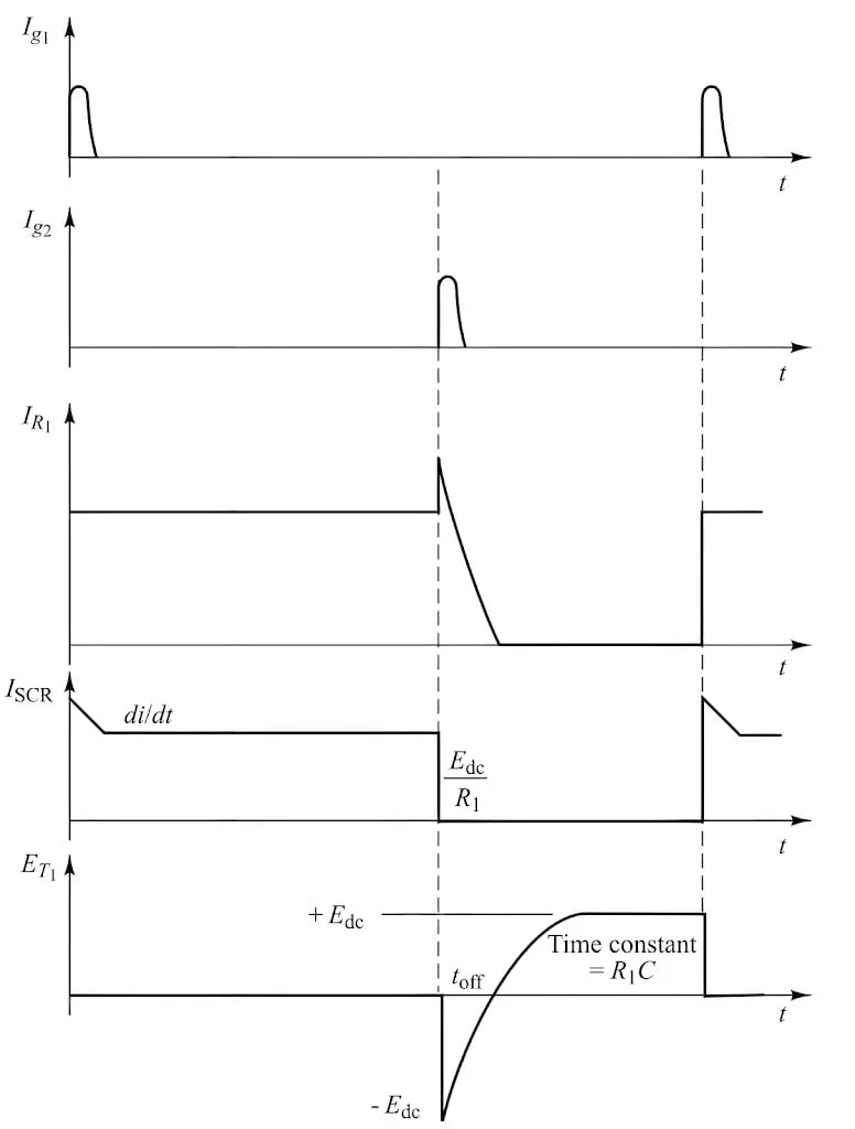
- When a triggering pulse is applied to the gate of `T_1`, the thyristor `T_1` is triggered. Therefore, two circuit current, namely, load current `I_l` and charging current `I_c` start flowing. Their paths are,
- Capacitor C will get charged by the supply voltage `E_{dc}` with the polarity shown in Fig. 7. The states of circuit components becomes,
3.Mode 2
- When the gate receives a triggering pulse,`T_2`turns on.As soon as `T_2` . As soon as `T_2` conducts, capacitor C applies its negative polarity to the anode and positive polarity to the cathode of `T_1`.This action creates a reverse voltage across the main thyristor `T_1` and immediately turns it off.
- Charging of capacitor C now takes place through the load and its polarity becomes reverse. Therefore, charging path of capacitor C becomes,
- Hence, at the end of Mode 2, the states of the devices are
4.Mode 3
- Now, when the circuit triggers thyristor`T_1` ,the capacitor discharges and forces the complementary thyristor `T_2` to turn OFF.This action completes Mode 3 and establishes the final state of the circuit,
- Therefore, this Mode 3 operation is equivalent to Mode 1 operation.
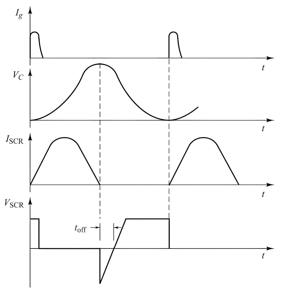
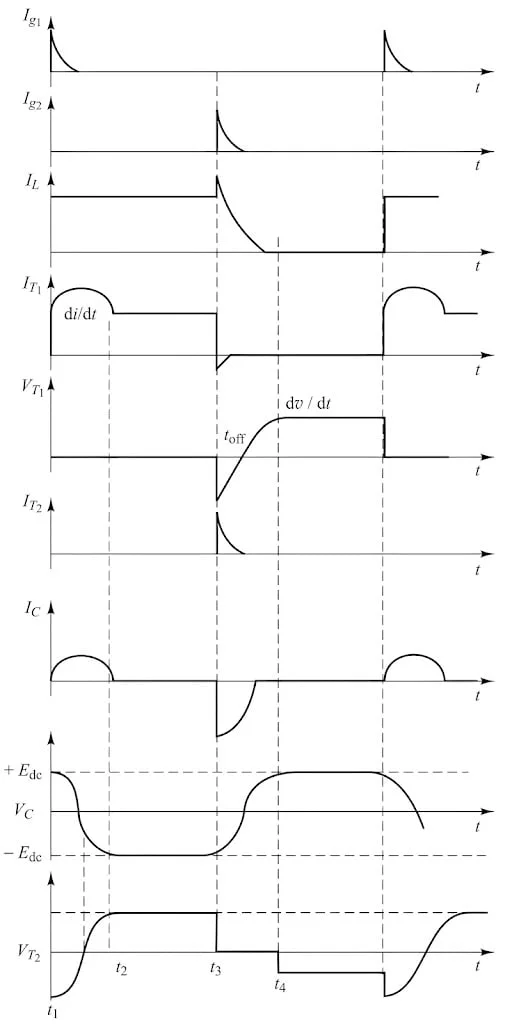
- Figure 8 shows the waveforms at various points in the commutation circuit. Engineers commonly use this class of commutation in the well-known McMurray-Bedford inverter. By incorporating specific accessories, they successfully apply this method at frequencies below approximately 1000 Hz. This technique also ensures sure and reliable commutation.
4.Class D—Auxiliary Commutation (An Auxiliary SCR Switching a
Charged Capacitor)
- Figure 9 shows the typical Class D commutation circuit. In this method, an auxiliary thyristor (`T_2`) commutates the main thyristor (`T_1`), Assuming ideal thyristors and lossless components, Figure 10 shows the corresponding waveforms. The inductor L ensures the capacitor C maintains the correct polarity.
- Thyristor `T_1` and load resistance RL form the power circuit, whereas L, D and `T_2` form the commutation circuit.
1.Mode 0: [Initial Operation]
- When you connect the battery `E_{dc}`,no current flows because both thyristors remain OFF. Hence, the initial state of the circuit components reflects this non-conducting condition.
2.Mode 1
- Initially, SCR `T_2` must be triggered first in order to charge the capacitor C with the polarity shown. This capacitor C has the charging path `E_{dc}`+-`C_+`-`C_-`-`T_2`-`R_l`-`E_{dc}`. As soon as capacitor C is fully charged, SCR `T_2` turns-off.
- This is due to the fact that,as the voltage across the capacitor increases, the current through the thyristor `T_2` decreases since capacitor C and thyristor `T_2` form the series circuit.Hence the state of circuit components at the end of Mode 1 becomes,
3.Mode 2
- When thyristor `T_1` is triggered, the current flows in two paths.
- After capacitor C completely discharges, its polarity reverses—the upper plate acquires a negative charge, and the lower plate acquires a positive charge. The blocking diode D prevents capacitor C from discharging in reverse.
- Therefore, at the end of Mode 2, the state of the circuit components becomes,
4.Mode 3
- When the thyristor `T_2` is triggered,capacitor C starts discharging through the path `(C_+)-T_{2left(a kright)}-T_{1left(k-aright)}-(C_-)`.When this discharging current (commutating current `I_c`) becomes more than the load current `I_l`,thyristor `T_1` gets OFF.
- Therefore, at the end of Mode 3, the state of circuit component becomes,
- Again, capacitor C will charge to the supply voltage with the polarity shown and hence SCR `T_2`gets OFF.Therefore, thyristors `T_1` and `T_2` both get OFF,which is equivalent to Mode 0 operation.
- This commutation circuit offers great versatility because it readily incorporates both time ratio and pulse width regulation. The system transfers commutation energy directly to the load, enabling high efficiency. Engineers often use this method in Jones chopper circuits.
5.Class E—External Pulse Commutation
- In the Class E commutation method, an external pulse source applies a reverse voltage to the current-carrying thyristor. Figure 11 shows a typical Class E commutation circuit, and Figure 12 displays the associated waveforms. In this setup, the commutating pulse reaches the circuit through a pulse transformer, which engineers design with tight coupling between the primary and secondary windings.
- Designers also include a small air gap in the transformer to prevent saturation when a pulse reaches its primary. The transformer carries the load current with only a small voltage drop compared to the supply voltage. To commutate T₁, the system applies a pulse whose duration matches or slightly exceeds the thyristor’s specified turn-off time.
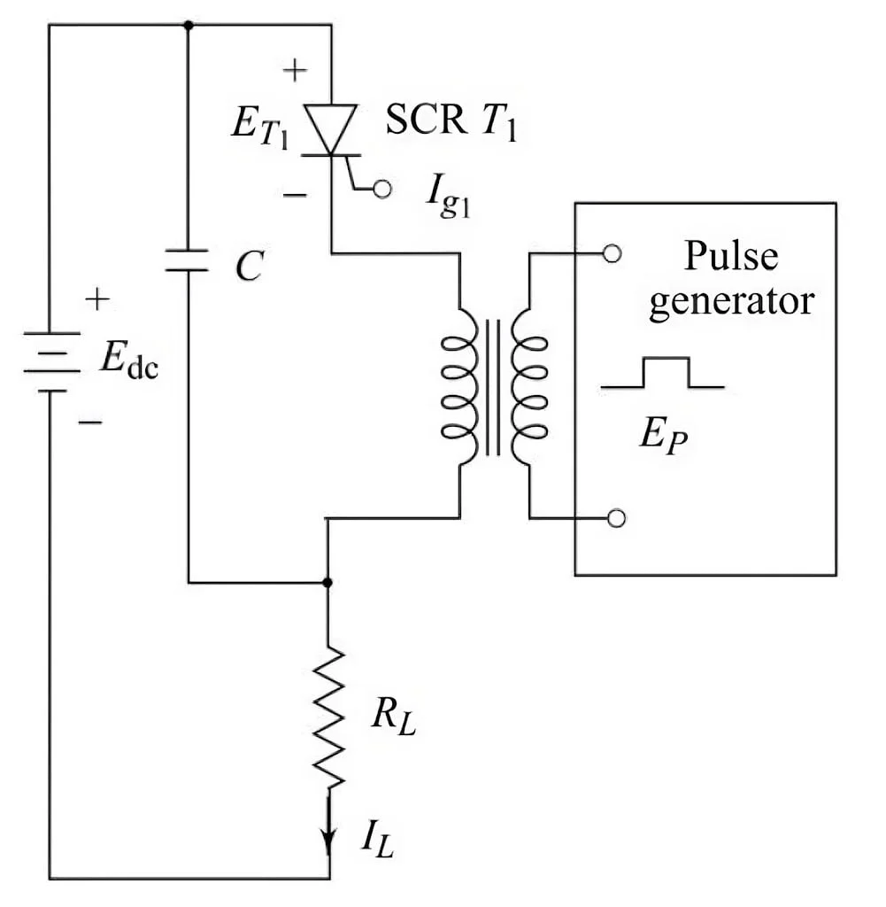
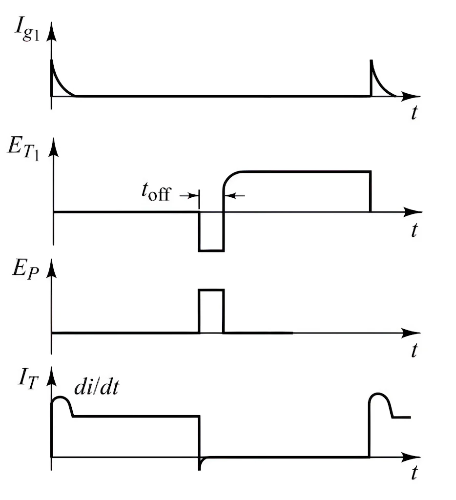
- When the circuit triggers SCR T1, current flows through the load RL and the pulse transformer. When the pulse generator applies a voltage pulse EP to the primary winding of the pulse transformer, the transformer induces a reverse voltage across thyristor T1, which immediately turns it off. Because this induced pulse has a high frequency, the capacitor presents nearly zero impedance. After T1 turns off, the load current drops to zero. Before the commutation, the capacitor maintains a low voltage of approximately 1 V.
- This commutation method delivers very high efficiency because it requires minimal energy and allows easy incorporation of both time ratio and pulse width regulation. However, equipment designers often overlook this method when designing power circuits.
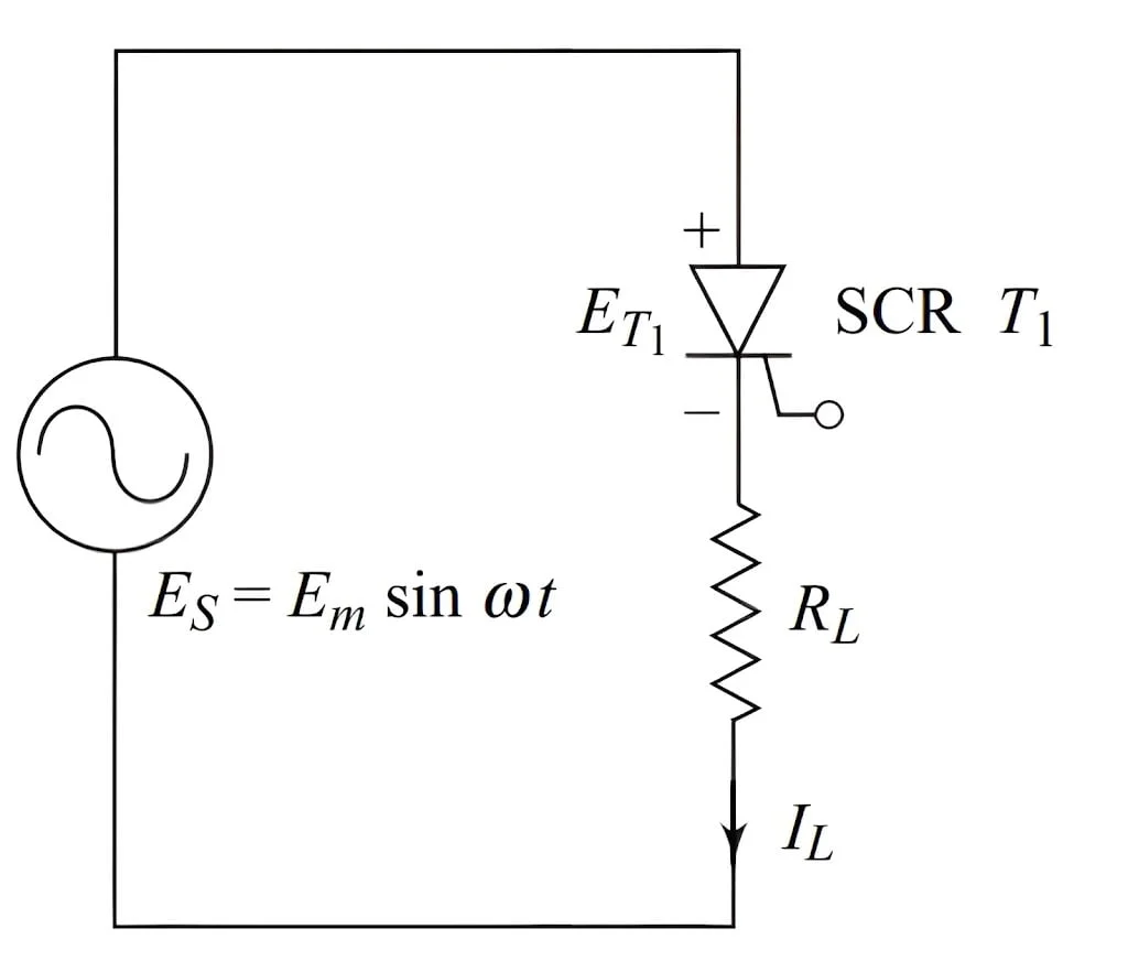
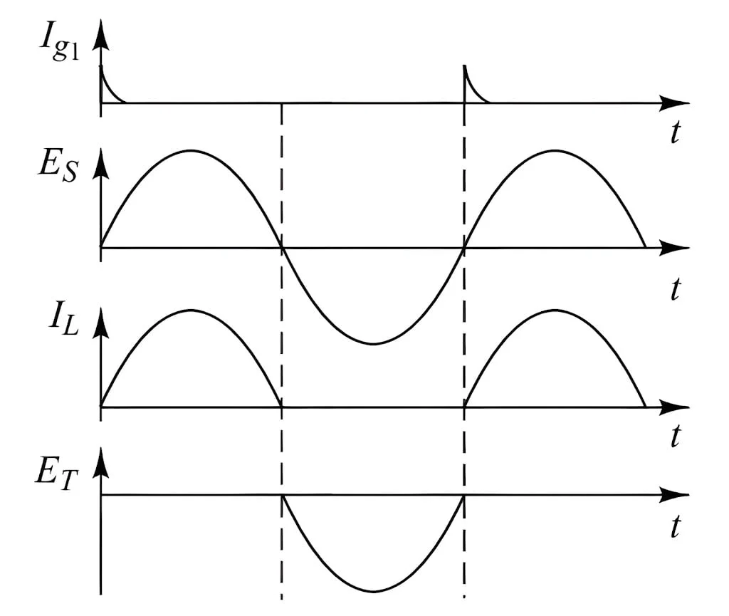
6.Class F—a.c. Line Commutation
- Figure 13 shows a typical line-commutated circuit, and Figure 14 displays its associated waveforms. When the supply delivers alternating voltage, the load draws current during the positive half cycle. During the negative half cycle, the negative polarity across the SCR turns it off.
- The duration of the half cycle must be longer than the turn-off time of the SCR. The maximum frequency at which this circuit can operate depends on the turn-off time of SCR.
Applications of Thyristor Commutation
Motor Control Systems
Power Supplies
HVAC and Heating Systems
Power Factor Correction (PFC)
High-Power Electronics
Welding Equipment
Frequency Converters and Inverters
Important Characteristics of Thyristor Commutation
To understand commutation fully, we must consider certain characteristics:
1. Turn-Off Time (tq)
The minimum time required for the thyristor to regain its blocking capability after current becomes zero.
2. Holding Current
The minimum current required to keep the thyristor in the ON state. If current falls below this level, the device turns off.
3. Reverse Recovery Time
The time required to remove stored charge carriers after conduction.
4. dv/dt Rating
Maximum rate of rise of voltage that the thyristor can withstand without turning on unintentionally.
5. di/dt Rating
Maximum rate of rise of current during turn-on to prevent device damage.
Conclusion
Overall, thyristor commutation is crucial for regulating power flow, switching devices, and maintaining effective operation in various electrical and electronic systems. Engineers, designers, and researchers in power electronics and electrical engineering must comprehend different commutation methods, characteristics, and applications for their work. Advancements and innovations in thyristor commutation technologies will improve power electronic performance, efficiency, and reliability as research and development progress.