Introduction
The SCR is one of the most important semiconductor devices used in modern power electronics systems. Engineers rely on this device to control electrical power accurately in many industrial and electronic applications. The SCR operates as a controlled switch that can handle high voltage and large current levels while maintaining reliable performance. Because of its special switching characteristics the SCR appears in motor controllers industrial automation systems heating equipment power supplies and many other electrical installations. Understanding the structure operating principle and characteristics of the SCR helps engineers design efficient electrical systems and manage electrical energy with precision in modern technology.

Understanding the Silicon Controlled Rectifier SCR
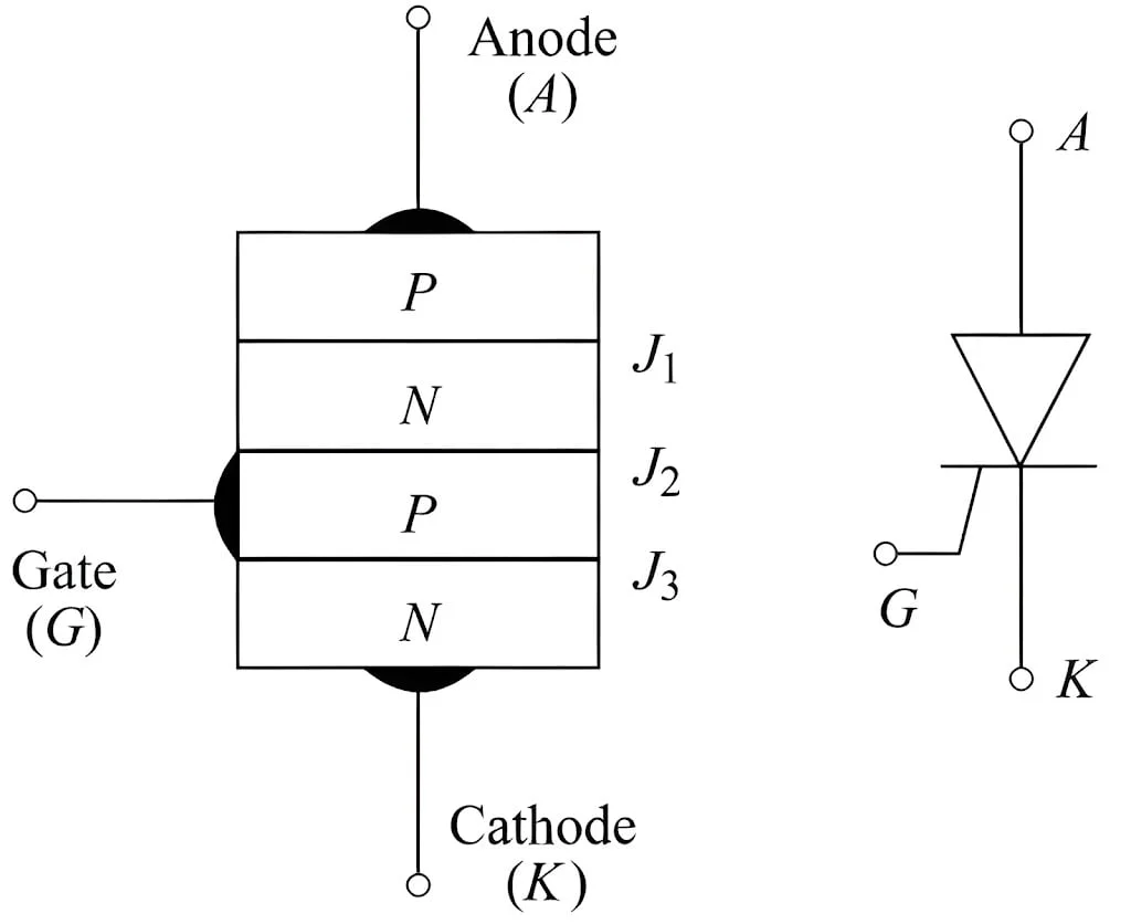
The Silicon Controlled Rectifier belongs to a group of semiconductor devices called thyristors. These devices function as controlled electronic switches that can conduct large currents once activated. The SCR contains four semiconductor layers arranged in a PNPN structure. Three internal junctions appear inside the device and these junctions control how electrical current flows through the component.
Engineers describe the SCR as a bistable device because it can exist in two stable operating states. In the OFF state the device blocks current even when voltage is applied across its terminals. In the ON state the device conducts current freely and behaves like a closed electrical switch. This switching behavior allows the SCR to regulate electrical power with high efficiency.
The SCR contains three external terminals known as anode cathode and gate. The anode connects to the positive side of the power circuit while the cathode connects to the negative side. The gate terminal controls the switching operation. A small gate current triggers the device and allows large current to flow between anode and cathode.
Historical development of the SCR
The development of the SCR marked a major advancement in semiconductor technology. Before the introduction of semiconductor switches engineers relied on mechanical relays or vacuum tube devices to control electrical power. These earlier technologies required larger equipment and offered limited reliability.
The SCR introduced a solid state solution that allowed fast switching and high power handling within compact devices. Engineers could control industrial motors heating systems and power supplies using electronic circuits rather than mechanical switches.This innovation transformed power electronics and opened the path toward modern electrical control systems used in factories energy systems and consumer electronics.
Basic structure of the SCR device
The SCR contains four semiconductor layers arranged in alternating P type and N type regions. These layers form three PN junctions labeled `J_1`, `J_2`, and `J_3`. The outer P layer connects to the anode terminal while the outer N layer connects to the cathode terminal. The gate terminal connects to the inner P region near the cathode.This layered structure allows the device to control the movement of charge carriers through the semiconductor material. When voltage appears across the anode and cathode the junctions determine whether current flows or remains blocked.The PNPN arrangement also allows the device to behave like two transistors connected together. A PNP transistor and an NPN transistor interact through regenerative feedback which allows the SCR to switch rapidly from non conducting state to conducting state.
Two transistor analogy of SCR
Engineers often explain SCR operation using the two transistor model. In this representation the four layer PNPN structure forms a pair of interconnected transistors. One transistor behaves as a PNP device while the other behaves as an NPN device.When gate current enters the device it triggers one transistor which then activates the other transistor through regenerative feedback. This feedback process rapidly increases current flow through the device.The interaction between these two internal transistor actions causes the SCR to latch into the conducting state once triggered. After this transition the device remains ON even if the gate signal disappears.
Terminals of the SCR
The SCR contains three external terminals that connect the device to electrical circuits. Each terminal plays a specific role in device operation.
- Anode terminal connects to the positive side of the power circuit.
- Cathode terminal connects to the negative side of the circuit.
- Gate terminal receives a control signal that triggers conduction.
The anode and cathode terminals carry the main current through the device. The gate terminal carries only a small control current that activates the switching action.
Working Principle of SCR
The working principle of the SCR depends on the behavior of its three internal junctions and the control signal applied to the gate terminal. Under different voltage conditions the device may operate in blocking mode or conduction mode.
When the anode becomes positive with respect to the cathode junctions `J_1` and `J_3` become forward biased. Junction `J_2` remains reverse biased which prevents significant current flow. In this condition the SCR remains in a non conducting state called the forward blocking state.
Only a small leakage current flows through the device during this stage. The depletion layer at junction `J_2` blocks most charge carriers from crossing the junction.When a gate signal is applied electrons enter the inner region of the semiconductor structure. This injection of carriers reduces the barrier at junction `J_2`. Once sufficient carriers appear the device enters the conduction state and current flows between anode and cathode.
Forward blocking condition
In the forward blocking condition the anode receives positive voltage relative to the cathode while the gate remains inactive. Junctions `J_1` and `J_3` allow current flow while junction `J_2` blocks the conduction path.The SCR behaves like an open switch during this condition. Only small leakage current flows through the semiconductor material.This blocking capability allows engineers to apply voltage across the SCR without activating the load circuit.
Triggering process through gate signal
The gate terminal allows engineers to trigger the SCR intentionally. When a small gate current flows between gate and cathode the internal carrier concentration increases.This increase reduces the depletion barrier at junction `J_2`. Once the barrier collapses regenerative feedback begins inside the PNPN structure.The SCR rapidly switches from blocking state to conduction state and begins carrying large current.
Avalanche breakdown and breakover voltage
If the anode to cathode voltage rises without gate activation the device eventually reaches the forward breakover voltage labeled `V_{BO}`. At this voltage the junction `J_2` experiences avalanche breakdown.The breakdown allows large numbers of charge carriers to cross the junction and initiate conduction. This process triggers the SCR even without a gate signal.Engineers normally avoid this method because it produces uncontrolled switching. Gate triggering offers more reliable control.
Latching behavior of SCR
Once conduction begins the SCR remains in the ON state even if the gate current disappears. This behavior occurs because the internal regenerative feedback maintains carrier flow between the two transistor regions.The device continues conducting until the anode current drops below the holding current value.This latching property allows the SCR to function as a stable electronic switch for power control systems.
Characteristics of SCR

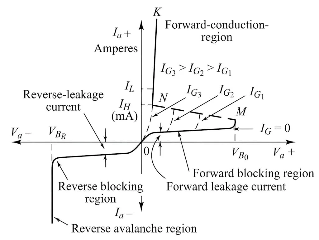
Reverse blocking region
In the reverse blocking region the cathode becomes positive relative to the anode. Junctions `J_1` and `J_3` become reverse biased while junction `J_2` becomes forward biased.Current cannot flow through the device because two junctions remain reverse biased. The SCR behaves like a reverse biased diode during this stage.If reverse voltage rises above the reverse breakdown voltage `V_{BR}` avalanche breakdown may occur which allows large reverse current.
Forward blocking region
In the forward blocking region the anode remains positive relative to the cathode but the gate signal is absent. Junctions `J_1` and `J_3` remain forward biased while `J_2` remains reverse biased.Only a small leakage current flows across the device during this stage. The SCR still behaves like an open switch.This state continues until a gate signal triggers the device or the forward voltage reaches breakover voltage.
Forward conduction region
Once triggered the SCR enters the forward conduction region. In this state the device conducts current with very low resistance.The voltage drop across the device decreases to about 1 to 2 volts even when large current flows.The SCR behaves like a closed switch and allows the load circuit to operate normally.
Applications of Silicon Controlled Rectifiers
The SCR appears in many electrical systems where controlled switching of high power is required. Its ability to handle high current and voltage makes it suitable for industrial power electronics.
- Motor Speed Control: Engineers use SCR devices in motor drive circuits to regulate speed and torque of electric motors.
- Power Supplies: SCR circuits regulate DC output voltage in controlled rectifier power supply systems.
- Heating Systems: Temperature control circuits in electric heaters and furnaces often rely on SCR switching.
- Light Dimmers: Lighting systems use SCR devices to regulate brightness in residential and commercial installations.
- Welding Equipment: Welding machines use SCR control circuits to manage current during welding operations.
- Power Factor Correction: Electrical systems use SCR circuits to improve power factor and reduce energy losses.
- High Voltage Transmission: HVDC transmission systems employ SCR devices to control high voltage power flow.
Conclusion
The SCR remains one of the most significant devices in modern power electronics because it provides reliable and precise control of electrical power in many industrial systems. Its PNPN structure regenerative switching behavior and strong current handling capability allow engineers to regulate high power circuits efficiently. Understanding the operating principle characteristics and applications of the SCR helps engineers design advanced electrical systems used in automation transportation manufacturing and energy distribution. Continuous research and technological development will further enhance SCR performance and support the growth of efficient power electronic systems.